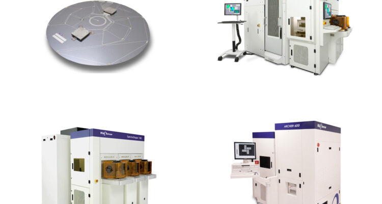
For advanced memory chip producers, KLA Corporation (NASDAQ: KLAC) today announced the availability of the ground-breaking Axion® T2000 X-ray metrology system. The accurate development of extraordinarily tall structures with deep, narrow holes and pits, as well as other sophisticated architectural patterns, requires control at the nanoscale level for 3D NAND and DRAM chip fabrication. Patented innovations in the Axion T2000 enable it to measure high aspect ratio device features with a previously unheard-of level of resolution, accuracy, precision, and speed. The Axion T2000 assists in ensuring the effective fabrication of memory chips used in applications like 5G, artificial intelligence (AI), data centres, and edge computing by identifying the minute shape irregularities that might affect memory chip performance.
According to Ahmad Khan, president of KLA’s Semiconductor Process Control business unit, “our new Axion T2000 X-ray metrology equipment is a game changer for inline process control during fabrication of sophisticated 3D NAND and DRAM devices.” “The Axion T2000 instantly creates a full 3D depiction of high aspect ratio structures on the order of 100:1 or higher using transmissive X-ray technology. Axion data enables careful control of crucial factors, such as breadth, form, and tilt, from the very top to the bottom of these extreme vertical features. Additionally, the Axion decreases the cycle time needed to resolve crucial yield and reliability concerns during large volume memory chip manufacture. This is because it measures inline.”
Source: Prnewswire


No Comments